
Physical Design Services
BroadSemi’s backend design team has a lot of experience with cutting-edge technology nodes, sophisticated architectures, and novel ideas. Our professionals give world-class assistance for the base stage of your product lifecycle, ensuring a substantially longer market stay with a significantly faster production, design, and fabrication cycle. At each step of the process, we squeeze time and cost with the help of our domain specialists.

Physical Design Services
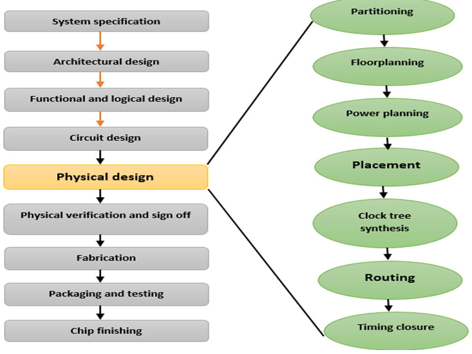
BroadSemi’s backend design team has a lot of experience with cutting-edge technology nodes, sophisticated architectures, and novel ideas. Our professionals give world-class assistance for the base stage of your product lifecycle, ensuring a substantially longer market stay with a significantly faster production, design, and fabrication cycle. At each step of the process, we squeeze time and cost with the help of our domain specialists. Especially, our engineers are mainly focusing on timing, power, logic equivalence, layout against schematic, on-chip variation, cross talk, and other physical verification checks are all performed. We achieve a controllable, high-performance, low-risk, and efficient physical implementation by ensuring seamless integration between physical design and design functions.
Skills & Expertise in the Physical Design:
BroadSemi’s Physical Design team has a diverse set of talents and experience that spans the full chip implementation process.
TOOLS:
- P&R Design flow: ICC, EDI, and Olympus toolset expertise. When needed, the team has also quickly ramped up on Atoptech and handled legacy MAGMA flows.
- STA: PTSI, ETS, Goldtime and some of the customer specific tools
- Power: Voltage Storm (now Voltus), Redhawk
- Physical Verification: Calibre, Hercules and some of the customer specific tools
- Scripting: Team comes with strength and attitude for automation. Strong in TCL (for ICC, EDI, MAGMA etc.), Perl, Make, SKILL and other utilities
- Analog layout: Virtuoso XL, HSPICE, Spectre
TECHNOLOGY NODE & FLOW EXPERTISE:
The team has tape-out experience on older nodes like as 40nm, 65nm, and also, most of the recent projects have been worked on 16nm, 14nm, and 28nm. Our technological competence, on the other hand, is distributed as follows:
- UPF/CPF based advanced low power flow
- MMMC/AOCV/POCV based High performance Flow
- Flat/Hierarhical, Abutted/Channel based module level design implementation flows
- Flipchip/ Wirebond implementation